DRV 8701
简介
DRV8701 是一款H桥门驱动器,可以驱动4个外部的N沟道mos管,允许有100%的PWM波占空比。DRV8701工作电压在5.9伏至45伏,根据型号的不同有两种控制接口,一种是PH/EN(DRV8701E),另一种是PWM(DRV8701P)。
DRV8701 具有5个等级的可调整门极驱动。
DRV8701 支持1.8V 3.3V 以及5V的逻辑输入电平。
综述
DRV8701是一款使用四个外部N沟道MOSFET的单H桥门驱动器,目标是驱动12-V至24-V双向有刷直流电机。
PH/EN(DRV8701E)或 PWM(DRV8701P)接口允许与控制器电路简单接口。内部感应放大器允许可调节的电流控制。门驱动器包括使用固定关断时间PWM电流斩波来调节绕组电流的电路。 DRV8701以9.5-V Vcs门驱动电压驱动高侧和低侧FET。所有外部FET的门驱动电流可通过IDRIVE引脚上的单个外部电阻器进行配置。
提供了一种低功耗睡眠模式,该模式关闭内部电路以实现非常低的静态电流消耗。通过将nSLEEP引脚拉低可以设置睡眠模式。 提供了内部保护功能: 欠压锁定、充电泵故障、过电流关闭、短路保护、预驱动故障和过温。故障情况通过nFAULT引脚指示。
note: 上面这一段是我从数据手册直接翻译的,嘻嘻
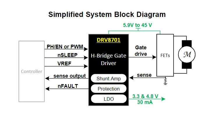
一个简要的系统框图如下所示
引脚配置和功能
| NAME | NO | TYPE | Logic | Description |
|---|---|---|---|---|
| EN | 14 | Input | Bridge enable input | 逻辑低电平将桥接电路置于刹车模式 |
| PH | 15 | Input | Bridge enable input | 控制H桥的方向 |
| NAME | NO | TYPE | Logic | Description |
|---|---|---|---|---|
| IN1 | 15 | Input | Bridge PWM input | Logic controls the state of H-bridge |
| IN2 | 14 | Input | Bridge PWM input | Logic controls the state of H-bridge |
| NAME | NO | TYPE | Logic | Description |
|---|---|---|---|---|
| VM | 1 | Power | Power supply | Connect to motor supply voltage; bypass to GND with a 0.1uF ceramic plus a 10-uF minimum capacitor rated for VM; additional capacitance may be required based on drive current |
| GND | 5,6,PPAD | Powerd | Device Ground | Must be connected to ground |
| VCP | 2 | Power | Charge pump output | Connect a 16-V, 1uF ceramic capacitor to VM |
| CPH | 3 | Power | Charge pump switching nodes | Connect a 0.1uF X7R capacitor rated for VM betweenn CPH and CPL |
| CPL | 4 | Power | Charge pump switching nodes | Connect a 0.1uF X7R capacitor rated for VM betweenn CPH and CPL |
| DVDD | 8 | Power | Logic regular | 3.3V logic supply regulator; bypass to GND with a 6.3V, 1uF ceramic capacitor |
| VDD | 7 | Power | Analog regular | 4.8V analog supply regulator; bypass to GND with a 6.3V, 1uF ceramic capacitor |
| nSLEEP | 13 | Input | Device sleep mode | Pull logic low to put device into a low-power sleep mode with FETs High-Z; internal pulldown |
| IDRIVE | 12 | Input | Gate drive current setting pin | Resistor value or voltage forced on this pin sets the gate drive current |
| VREF | 6 | Input | Analog reference input | Controls the current regulation; apply a voltage between 0.3V and AVDD |
| nFAULT | 9 | Open Drain | Fault indication pin | Pulled logic low with fault condition; open-drain output requires an external pullup |
| SNSOUT | 10 | Open Drain | Sense comparator output | Pulled logic low when the drive current hits the current chopping threshold; open-drain output requires an external pullup |
| SO | 11 | Output | Shunt amplifier output | Voltage on this pin is equal to the SP voltage times plus an offest; place no more than 1 nF of capacitance on this pin |
| SN | 20 | Input | Shunt amplifier nagative input | Connect to SP through current sense resistor and to GND |
| SP | 21 | Input | Shunt amplifier positive input | Connect to low-side FET source and SN through current sense resistor |
| GH1 | 17 | Output | High-side gate | Connect to high-side FET gate |
| GH2 | 24 | Output | High-side gate | Connect to high-side FET gate |
| GL1 | 19 | Output | Low-side gate | Connect to low-side FET gate |
| GL2 | 22 | Output | Low-side gate | Connect to low-side FET gate |
| SH1 | 18 | Input | Phase node | Connect to high-side FET gate source and low-side FET drain |
| SH2 | 23 | Input | Phase node | Connect to high-side FET gate source and low-side FET drain |
细节描述
Overview
DRV8701是一款H桥门驱动器(也称为预驱动器或控制器)。该设备集成了FET门驱动器,以控制四个外部NMOS FETs。设备可以在5.9伏到45伏的供电电压下工作。
简单的PH/EN(DRV8701E)或PWM(DRV8701P)接口允许与控制器电路进行连接。包含一个低功耗睡眠模式,可以通过nSLEEP引脚启用。
门驱动强度可以调节,以优化系统对给定FET的性能,无需在FET门上添加外部电阻。IDRIVE引脚允许选择注入外部FET门的峰值电流。当VM大于12V时,高侧和低侧FETs通常以9.5V的Vcs电压驱动。在较低的VM电压下,Vcs会降低。高侧门驱动电压是使用双倍架构的充电泵产生的,调节到VM + 9.5V。
该设备通过将必要的FET驱动电路集成到单一设备中,极大地减少了离散电机驱动系统的组件数量。此外,DRV8701增加了传统离散实现之外的保护特性:欠电压锁定(UVLO)、过流保护(OcP)、预驱动器故障和热关闭。
内置了使用固定时间关断电流斩波方案的启动(冲击)或运行电流限制。斩波电流水平是通过选择感应电阻值和设置VREF引脚上的电压来设定的。
提供了一个分压放大器输出,供系统控制器进行精确的电流测量。SO引脚输出的电压是感应电阻上电压的一半。